3D Printing Assisted Fabrication of Soft Robotic Hand with Embedded Soft Electronic Circuits
Introduction
Despite the recent advancements in soft actuators and robots, integrating electronic functionalities into soft robotic systems remains a challenge. Particularly, a direct combination of conventional, rigid electronic components such as copper wires and soft robotic parts poses numerous problems with structural integrity and stability. This is because the mechanical property mismatch between the rigid electronic components and soft body generates points of stress concentration at the interface that typically becomes initiation points for failure during operations. Among possible solutions, developing soft conductors with comparable mechanical property to the soft robotic body seems to be a promising direction of development. However, although several types of inherently stretchable conductors have been developed for various sensors and electronic applications, functional incorporation of such materials into soft robotic systems tends to be tough. In this project, we present a two-step fabrication process that comprises of 3D printing a soft electronic circuitry on a soft base followed by an assembly with a molded soft robotic body. We demonstrate that the proposed approach can successfully fabricate a soft robotic hand with embedded soft electronic circuits, which can also light LEDs.
This project was performed by Pelkins Ajanoh and Jane Im. Pelkins majors in mechanical engineering at MIT, while Jane majors in computer science at Korea University, and is currently a special student at MIT. The team was supervised by Hyunwoo Yuk, a research assistant at MIT SAMs Lab.

|
Objectives
The project’s objective is to demonstrate a facile method of embedding printable electronics into a pneumatically actuated soft robotic hand. In addition, the project aims to present a two-step fabrication process comprising of a combination of conventional mold-based fabrication of the soft robotic body and 3D printing of soft electronic circuitry.
We will describe the fabrication approach of molding and 3D printing in a step-by-step manner. We will also discuss the rationale behind the choice of conductive ink, and preparation of the soft electronic circuit. We will further demonstrate the design process and implementation of our proposed fabrication tactics for the miniature soft robotic hand, capable of accurately controlled gripping and flexing motion. The hand will have an embedded LED lighting circuit that will illustrate how the conductive material can be used.
We hope that the proposed method in this project will serve as a guide for those interested in embedding electronics in soft robots as well as those interested in exploring different fabrication methods like molding and 3-D printing in soft robotics.
Design
Design strength and weakness
Strength
The main strength of the soft robotic hand is structural integrity and stability. Mechanical property mismatch between soft body and rigid electronic components often causes stress concentration, but since the soft robotic hand contains a 3D printed circuit instead of electronic wires these problems are prevented.
Another major strength of the robotic hand is the aesthetics. Due the absence of rigid electric wires on the robot's external surface, the overall structure more closely resembles a child's hand. Overcoming the issue of integrating the two layers (see Troubleshooting - 2. Integration of layers) also contributed to making a more elegant looking human hand, because it meant no adhesive material had to be plastered in between both layers, which previously led to uneven surfaces and air leakages.
Weakness
One major weakness of the soft robotic hand is that the design does not support intricate movements, such as playing the piano or writing words using a pencil. The most the hand can do is grab objects up and down.
Another major weakness is that the lighting of LEDs is not synchronized with the fingers' motion, which was another goal of this project. If we were to do another iteration, our team would have added the function of lighting up the LEDs based on fingers' movements.
Layers
There are two layers in total.
The first, thick layer is the main body, while the second, thin layer (base) has conductive material and LED embedded into it.

|

|
The pictures above were taken during the proof-of-concept stage of the project. The final version of the hand robot is shown below.

|
Mold
Overall Design
The mold design showed below is for the main body of the hand which will be filled with polydimethylsiloxane. During the first iteration, we made molds of each of the fingers and tried to combine the solidified polydimethylsiloxane(pdms) from each of the molds together into the hand, but that didn't work. So we decided to design a single mold of all the fingers.
Each finger has extruded pieces for making channels and chambers, with extruded long lines for air channels being connected all the way to the end of the hand, where they will be connected to the pipes and pump. It is important for the air channels to be high enough (at least a quarter of the total height of the fingers) for smoother actuations.

|
The file for printing the mold was made using SolidWorks. The STL can be downloaded on this page.

|

|
Braces Using Later Cutting
After the mold was printed, we added 'braces' in each finger to separate each of the chambers and to facilitate actuation. The 'braces' were made by drawing 0.44' x 0.20' rectangles with the CoreIDRAW X5 and laser-cutting 2 mm thick Poly (methyl methacrylate) (acrylic) sheets with the Epilog Laser Mini.

|

|
More details are described in 3) Fabrication- Step 2
Conductive Material Layout
Each finger has an LED on its fingertip and the LEDs are connected to the conductive material. After troubleshooting, the final layout of the circuitry is shown below.
The LEDs' negative terminals are each connected to a line that is printed along each finger, and all five lines are then connected together to a single ground. The positive terminal of the LEDs are connected on one line (the red line) which takes a shape of the hand's outline.

A simple drawing of the final layout of the conductive material.

|
|

|
|
| Actual 3D printed conductive material |

Fabrication
Bill of Materials
The file below contains the materials needed for this project and the cost of each.
| 3d_printing_embedded_conductive_bill_of_materials.xlsx | 9 KB |
Step 1: Making the Mold
3D Printing the Mold
For 3D printing the mold, we used Form2 of Formlabs with Clear Resin.

The software that we used was PreForm. In order to print in a short time, the orientation of the mold needs to be adjusted so that it sticks directly to the top of the printer without being supported by scaffolds.


After the 3D printing process is finished, take out the material and rinse it in ethanol.

Ensure complete curing of the mold using UV curing machine
Step 2: Molding: Making the Main Body
Making the Main Material
The material used was Polydimethylsiloxane (PDMS). We used the product Econ® 80 (80A Urethane Rubber Compund) from company Smooth-On Inc.

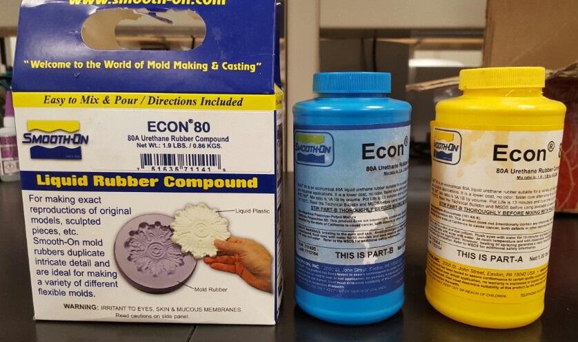
There are two liquid parts A and B. First, we stirred each part thoroughly with a stick.
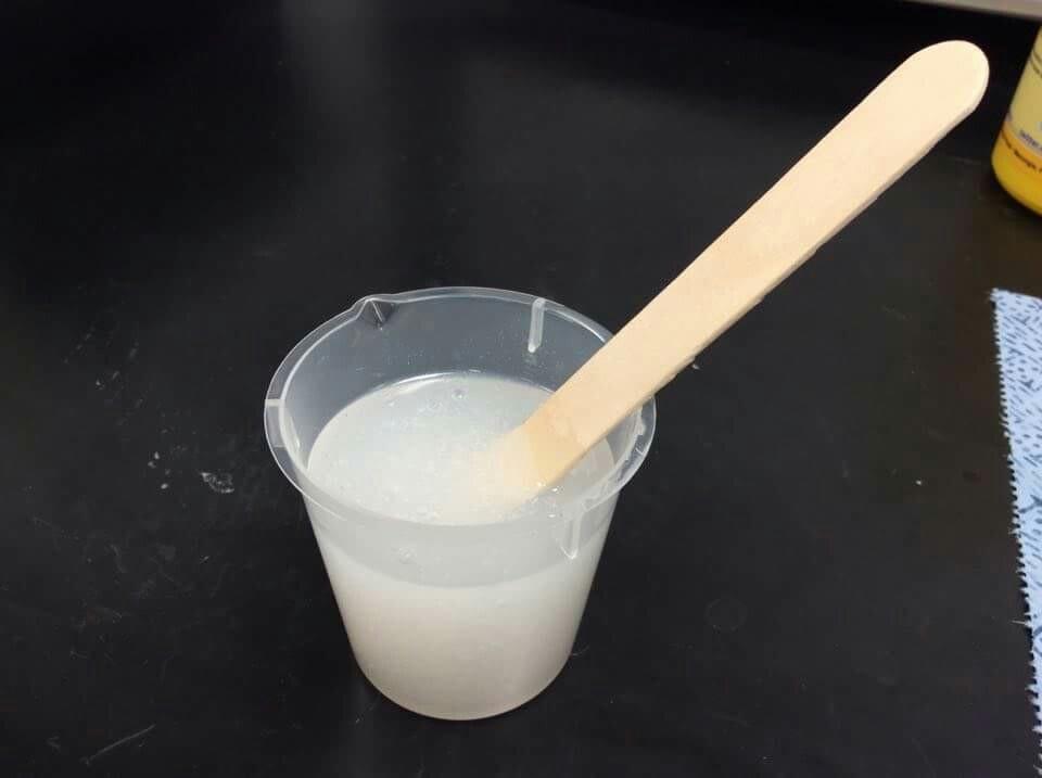
After each part was sired, we mixed A and B in a 1:1 ratio by volume. It is okay to mix with a stick as long as it is mixed thoroughly. After the mixing, we could see air bubbles inside the material. The next step was vacuum-degassing to get rid of the air bubbles.
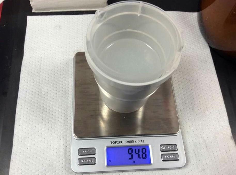
To minimze air bubbles in cured rubber, it is important to do vacuum degassing. Before we used the conditioning mixer, we first measured the weight of the material, the cup that contained the material, and the container used for the mixer.
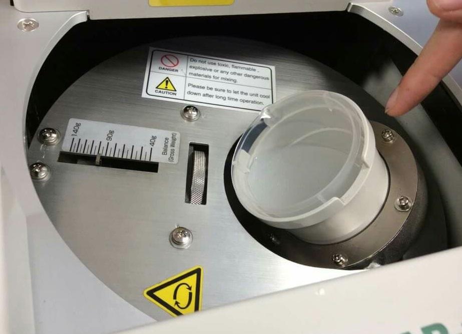
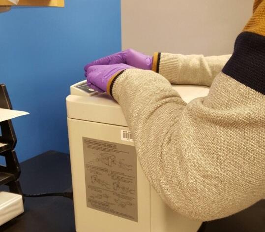
We used a conditioning mixer called AR-100. Since the weight was 94.8g, we adjusted the weight condition accordingly, and de-foamed it.
Laser Cutting the Braces
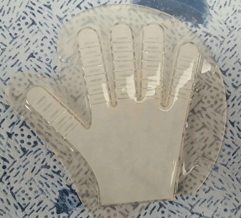
In order to enable the fingers to be bent easily, small cracks should be made in the fingers. For this, small rectangular pieces (which we called "braces") were put within the finger parts of the mold.

|

|
Using CoreIDRAW X5, we drew 0.44' x 0.20' rectangles and sent them to the Epilog Laser Mini.
The Laser Mini was used to cut 2mm thick Poly (methyl methacrylate) (PMMA).

|
|
After de-foaming, slowly pour the material in the mold.
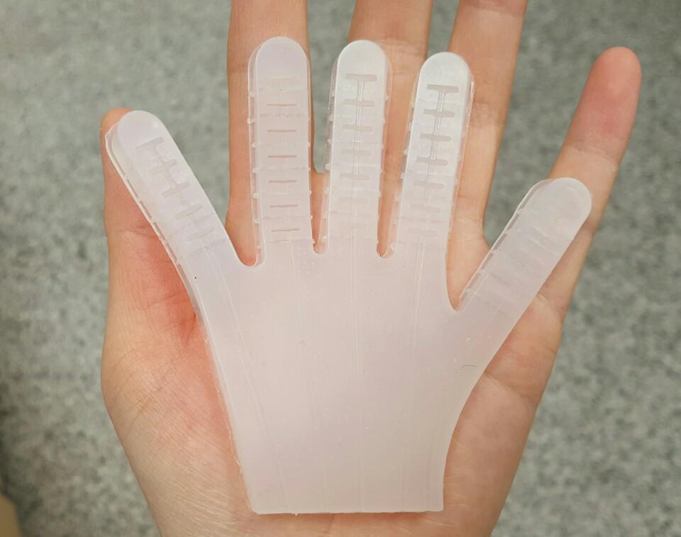
Cure overnight (at least 24 hours) at room temperature (73°F/23°C) and then demold.
After the mold hardens, add the laser cut braces on each finger.

Remove the braces after the polydimethylsiloxane has been cured.
Step 3: 3D Printing Conductive Material
Overall Process
In order to print the circuitry, we needed a 3D printer that was able to print precise, thin lines. The printer used was from MIT SAMs lab, of which the two team members contributed in assembling. We mounted the Aerotek three-axis gantry and used LabView to synchronize it with micro-dispensers.
To use the printer:
- First, turn on the controller implemented with LabView.
- Load the right code (the G-Code can be downloaded from the bottom of this page).
- Adjust the board so that it isn't far way from the ink source
- After the printing, scrape off some ink that deviated from the path with a pincette.

It is important to adjust the distance between the board and the ink source before printing.

More details can be found in the "Video of Printing" section.

After printing, scrape off some ink deviated away from the path with a pincette.
Precaution
The following precautions seem trivial, but are crucial in order to make good quality printing.
- Constantly check if the print runs out of ink, or if there is too much ink.
- Make sure there is no air bubbles (gas) inside the ink.
Material used for printing
The material used for printing is a stretchable silver conductor called ME603, produced from DuPont. ME603 was chosen because its conductivity is maintained even after being cured in 100 degrees with PDMS poured over it. It withstands thermoforming and over molding temperatures.
Video of Printing
|
|
Code
The G-Code used for printing is in the attached files downloaded on this page.
Step 4: Preventing Air Channels from Being Blocked
In Step 5, the base (thin layer) containing conductive material) and the main body was integrated together by placing the main body on the base and letting both cure. However, during this process, there is a danger of the air channels being blocked by the material of the base since it is still fluid and can flow into the channels. In order to prevent this, laser cut pieces were placed in the air channel before proceeding on to Step 5.
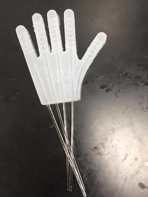
We used the same tools as in Step 2, under the subtitle, Laser Cutting the Braces, which are the CoreIDRAW X5, to sketch out the top view of the sticks and the Epilog Laser mini, to laser cut the 2 mm thick PMMA into four 9'X0.079' sticks. Each stick was placed in the air channel of each finger as in the image above.
Step 5: Making Base Integrated with Conductive Material
Making the material
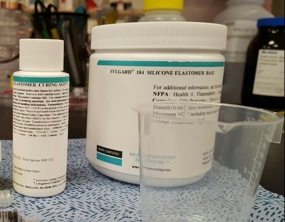
The material used for the base was SYLGARD® 184 SILICONE ELASTOMER KIT from Dow Corning. The base (part A) and curing agent (part B) should be mixed with 10:1 ratio. To cure this material, it should be placed in a oven at 100 degrees for 35 minutes.
Place LEDs on the 3D printed circuit
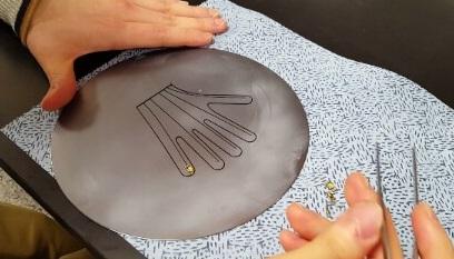
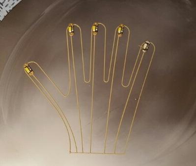
The 3D printed conductive material will serve as circuits needed for the LED to light up. Place one LED on each fingertip.
Pour PDMS on the printed conductive material
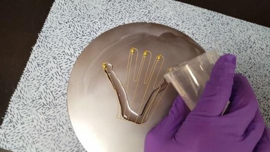
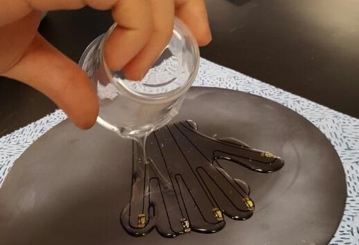
Slowly pour the PDMS that have been prepared. Make sure the it is spread evenly.
Place the main body onto the poured PDMS
Place the main body (that is prepared in Step 4 with laser cut PMMA sticks) over the PDMS that is just poured onto the circuit, with the air channels facing the PDMS, and let both layers cure and bond to form a single part. Make sure the PMMA sticks do not fall out of the air channels, since they are needed to prevent the PDMS filling in the air channels.
Step 6: Setting Up Control Board
Setting up Control Board
For the control board, we used the Fluidic Control Board of Soft Robitcs Toolkit.

Video of Testing
|
|
Troubleshooting
There were many troubleshooting processes while deciding on the final design. This section will introduce major design issues and overall strength and weakness of the final version.
1. Two layers of conductive material
In the initial design, the hand robot had two thin layers for the conductive material, instead of one. Each layer consisted two different parts of the circuit, one that will be connected to the positive terminal and another that will be connected to the negative terminal of LEDs.
Below images show how the two thin layers are combined.

We made two thin layers, each with conductive material of different layouts embedded into it.

The two layers are integrated into one layer by pasting one to another using adhesive material made using DOW CORNING® SE 1700.

The final shape of the two layers integrated into one layer.
However, we soon figured out that we needed only one layer if we changed the circuit. Having only just one layer for the conductive material saved time because it meant we only needed one 3D printing process, and did not have to make an adhesive material to combine the two layers into one. Therefore, in the final version we only made one layer for the conductive material which is shown as following.

Final one layer with different circuit.
2. Integration of layers
A tricky problem our team had to overcome was integrating the two layers described in section 2)Design - 1.Overall Layers, which are 1. main thick body and 2. thin layer containing 3D printed conductive material and LEDs.
We first tried pasting the thin layer onto the thick body by using DOW CORNING® SE 1700.
Below are images showing the process.

Process of pasting the adhesive material made from DOW CORNING® SE 1700 onto the thin layer.

Process of pasting the thin layers onto the main body.

Adhesive material mainly being plastered in the sides, in order to prevent air escaping from channels.
However, it was soon found out that while pasting the sticky material onto the base, some air channels would get blocked easily. This was mainly due to the size of the hand. Due to the hand being very small like a child's hand, some adhesive material inevitably got smudged onto the air channel during the process.

Tearing the thin layer revealed that the adhesive material are also smudged onto the air channel.
Another problem was that the adhesive material had to be pasted all over the sides of the hand in order to firmly combine the layers, causing the hand's surface to be rough and bumpy due to remains of the adhesive material. Although this was not a major problem, it certainly was undesirable from the perspective of user interface.

To solve this problem, we decided not to paste the layers together but cured the thin layer while the main body was on top of it. The process will be described in 3) Fabrication - Step 5.
Final Version
Strength
The main strength of the soft hand robot is structural integrity and stability. Mechanical property mismatch between soft body and rigid electronic components often causes stress and strain concentration, but since the soft hand robot contains a 3D printed circuit instead of electronic wires these problems are prevented.
Another major strength of the hand robot is the interface. Due to no electric wires surrounding the robot's external surface, the overall interface also is more close to resembling a child's hand. Overcoming the issue of integrating two layers (Major Troubleshooting - 2. Integration of layers) also contributed to making a more sleek looking human's hand, because it meant no adhesive material has to be plastered onto it, which previously caused the surface to become bumpy.
Weakness
One major weakness of the soft hand robot is that the design does not support intricate movements, such as playing the piano or writing words using a pencil. In the final version, the hand robot was maximally tested whether it could grab an object and move it around.
Another major weakness is that the lighting of LEDs is not synchronized with the fingers' motion, which was another goal of this project. If we were to do another iteration, our team would have added the function of lighting up the LEDs based on fingers' movements.
Modeling
We ran an FEA analysis on Abaqus and after setting our boundary and flow conditions, we obtained the results shown in the attached video.
Video of FEA analysis
|
|
Testing
Images of Testing
All LEDs that are connected to the control board using the 3D printed circuit turn on normally.

Each individual finger bent based on the the action made on the control board. The hand can also perform more complicated motion, such as grabbing and moving objects. Videos of the hand during testing are featured below.
Videos of Testing
Basic bending motion
|
|
Grabbing motion
|
|
LED lighting with bending motion
|
|
30 second version video of the three above
|
|
FEA analysis
|
|
Downloads
The following files are:
- 3d_printing_embedded_conductive_bill_of_materials.xlsx: Bill of materials for fabrication of all components
- hand_circuit.txt : G-Code for 3D printing conductive material
- me603_description.pdf : Technical description about the material used for 3D printing
- main_layer.zip: Main layer mold stl
| 3d_printing_embedded_conductive_bill_of_materials.xlsx | 9 KB | |
| me603_description.pdf | 320 KB | |
| hand_circuit.txt | 22 KB | |
| main_layer.zip | 47 KB |
